
Our Features


Avalanche Noise Source Design
Motivation
A high quality noise source is necessary for any good cryptographic enclave. In fact, multiple high quality noise sources are preferable, if the budget allows.
On-die RNGs such as ring-oscillator based RNGs leverage the metastability of sampling circuits to translate timing jitter into a random stream of bits. These are area and power efficient but are also tricky to verify. They are particularly vulnerable to subtle mask-editing attacks.
In addition to an on-die RNG, Betrusted’s entropy pool is reinforced by an externally testable noise source. Avalanche noise sources fit the bill, as they can delivery reasonably high quality entropy and verification can be done using a low-end “economy” oscilloscope.
The challenges of avalanche noise sources include the need for high (10-30V) voltages (and correspondingly high power consumption), and there the amount of noise generated depends on subtleties such as the engineering of the PN junction and the ambient temperature. Here we discuss the design and implementation of an avalanche noise source suitable for integration into a low-power, small-footprint mobile device.
Avalanche Breakdown Theory
Readers who just want to skip to the design can safely jump over this section. However, few discussions of avalanche noise sources address the theory of the noise source, which is important to understand when trying to rationalize power and component selection. If you plan to adjust or tweak the design, it’s recommended you at least skim this section.
Avalanche breakdown is essentially a miniature particle accelerator, where electrons that enter a PN junction’s depletion region (through mechanisms that include thermal noise) are accelerated across an electrical field, to the point where new electron-hole pairs are generated when these high-energy electrons collide with atoms in the depletion region, creating an amplification cascade with low reproducibility.
An approximate analogy is an inflatable pool filled with water. The height of the pool is the potential barrier of the reverse-biased PN junction. A hose feeding water into the pool represents a constant current of electrons. The volume of the pool can be thought of as the depletion capacitance, that is, the capacitor created by the region of the junction that is void of carriers due to natural drift and diffusion effects. As water trickles into the pool, the water level rises and eventually forms a meniscus. Random disturbances, such as ripples on the surface due to wind, eventually cause the meniscus to crest over the edge of the pool. The water flowing over the edge pushes down on the inflatable pool’s side, causing more water to flow, until the level has reduced to a point where the inflatable pool’s side can snap back into its original shape, thus restarting the cycle of filling, cresting, and breakdown. The unpredictability of when and where the breakdown might happen, and how much water flows out during the event, is analogous to the entropy generated by the avalanche effect in a PN junction.
The electrical characteristic of avalanche noise biased by a constant current source is a “sawtooth” waveform: a linear ramp up in voltage as the capacitance of the depletion region charges to the point where the electric field becomes large enough to initiate the cascade, and then a sharp drop off in voltage as the cascade rapidly discharges the junction capacitance. The cascade then abruptly halts once the field is no longer strong enough to sustain the cascade effect, leading to a subsequent cycle of charging and breakdown.
Avalanche diodes are high voltage devices because of the physics behind them. The breakdown voltage of the junction is controlled by the doping levels of the P and N regions:
Vbr = (Ecr^2 * Esi / 2q) * ((Na + Nd) / Na * Nd)
- Ecr is the critical value of the electrical field, a physical constant that ranges from 210^5 V/cm to 810^5 V/cm depending on the doping
- Esi is the dielectric constant of silicon
- q is the elementary charge of an electron
- Na is the doping concentration of the P region
- Nd is the doping concentration of the N region
Vbr increases as the temperature increases: as temperature goes up, so does lattice vibrations. Electrons are thus more likely to be scattered before they can be accelerated to a sufficient momentum to initiate the avalanche cascade. Thus a given junction engineered for a fixed Vbr exhibits decreased noise at higher temperatures. When confirming the performance of an avalanche noise source, it’s therefore important to confirm its performance at the highest expected operating temperatures.
In order to engineer a low voltage breakdown, the doping Na and Nd must be so high that the depletion region shrinks to a distance on the order of 10nm, such that quantum tunneling becomes the dominant effect. Quantum tunneling is synonymous with the “zener” effect, and is a different physical process which generates less noise. Thus for reverse-breakdown junctions that operate below 4.5-6.5V, the process is predominantly a zener effect and not as suitable for noise generation. This explains why avalanche noise generators must operate at higher voltages.
Note that Vbr decreases as temperature increases for the zener effect, opposite the avalanche effect. Thus “zener diodes” sold for the purpose of voltage regulation are actually engineered to use a combination of quantum zener plus avalanche effects, as they have opposite temperature coefficients and can lead to a more temperature-stable voltage reference.
The hybrid engineering of the zener diodes has lead to some confusion when selecting suitable parts as an avalanche noise source. However, zener diodes above 7V or so start to rely more and more on avalanche breakdown, so one may more accurately call a high voltage zener diode an avalanche breakdown diode.
Note that avalanche diodes to be used as voltage references are engineered to be less suitable as a noise source. Obviously, if the goal of the Vbr is as a voltage reference, reduced noise is highly desired. Generally, noise can be reduced by operating the diode at a higher current: more carriers means more opportunities to initiate the avalanche cascade. However, simply cranking up the current would also waste power. Thus avalanche diodes engineered as a voltage reference are designed so that the junctions are “leaky” compared to a typical rectifier application – perhaps through a very large area junction, with trace amounts of minority carrier dopants added to seed reverse leakage. Increasing low-level reverse-bias leakage reduces avalanche noise at lower current levels, because the tiny leakage helps “seed” the avalanche effect more consistency.
Thus when evaluating devices, the following are positively correlated with increased noise generation:
- Higher breakdown voltage
- Lower leakage current in reverse bias
A variety of inexpensive zener regulators as well as ESD protection diodes meet this criteria. ESD protection diodes in particular care little about how much avalanche noise is generated, and may prioritize lower leakage in reverse bias instead.
NPN transistor junctions
A discussion of B-E junctions of NPN transistors as an avalanche noise source is warranted due to its popularity in inexpensive noise sources. B-E junctions are engineered with very heavy doping on the E side, and light doping on the B side. This causes a very narrow depletion region on the emitter, and a large depletion region on the B side. In this case Vbr is dominated by Na, e.g.:
Vbr ~ 1/Na
The heavier the emitter doping, the lower the Vbr. And emitters on NPN transistor are heavily doped, so Vbr tends to be in a the range of 5-12V. The low breakdown voltage and wide availability of NPN transistors thus makes the device appealing.
Unfortunately, the threshold between zener breakdown and avalanche isn’t a clear line; in fact, NPN transistors with breakdowns approaching the 5V range exhibit behavior closer to zener breakdown (quantum tunneling) and are thus less suitable as a noise source.
Furthermore, because NPN transistors are not well-characterized for their reverse B-E breakdown, the quality of the noise generated can vary widely between manufacturers and models. The Internet also contains anecdotes that over time the B-E junction “wears out” over a period months and the quality of noise degrades, but there is no discussion of mechanism or backup with measurements.
Circuit Design
Thus, the desired properties for the mobile-friendly avalanche noise circuit are:
- Constant current source, adjustable to uA-range
- High voltage compliance on the constant current source (to 30V+)
- Post-noise source amplification/signal conditioning
- Small footprint (<1 cm^2)
- Low active power (< 5mW)
- Standby mode
Fortunately, most of these requirements are met by a class of regulators meant for controlling LCD blacklights and/or white LEDs. Photonic flux of an LED is proportional to current (not voltage) and thus for consistent light output across a wide range of devices LED regulators are almost always constant current sources. The desire to stack multiple LEDs on top of each other means almost all of these devices have very high voltage compliance as well.
The TPS61158 is identified as one of many suitable devices, this one chosen because it has a voltage cap at 30V, and features reasonable standby power and quiescent current draw. There may be others with even better characteristics, but the search stopped with this part because it met the desired properties of the circuit.
The final configuration simply replaces the LED string with a PN junction in reverse bias, along with a resistor stacked above the PN junction to provide some voltage compliance for the noise to generate. The voltage compliance is pure resistive power loss, so we target around a 1-2V compliance voltage, as the anticipated noise voltage is around 500mVp-p.
The main risk point of the circuit is operation at extremely low currents; the circuit is normally specified to provide 20mA of current, and we are operating it around a few uA. The low current operation may lead to instability in the regulator control loop and cause problems with circuit startup, so this needs to be characterized carefully.
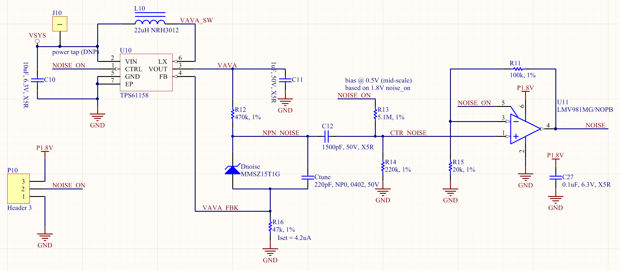
The cathode of the noise generator is AC-coupled to a resistive divider that centers the noise within the sweet spot of an amplifier that provides a 6:1 gain on the generated noise. More important than the voltage gain is the impedance matching to the sampling circuit. The noise generator runs at a very low current, and thus is incapable of driving any significant load. Thus even if the amplitude of the noise source was sufficient for direct sampling or use, a signal conditioning buffer of some sort would still be necessary to provide sufficient drive current for the ultimate circuit load. The target sampling circuit in this case is a 1MSPS 12-bit ADC with a 0-1V input range.
Circuit Characterization
Several devices were evaluated for their noise performance using the circuit as designed:
| Part number | Mfg | Vbr | noise mVpp | Type |
|---|---|---|---|---|
| MMBT2222A-7-F | Diodes Inc | 7.52 | 69.6 | NPN |
| MMBT3904LT1G | On semi | 7.8 | 80.4 | NPN |
| MMBT2484 | On semi | 10.65 | 571 | NPN |
| BSV52LT1G | On semi | 7.39 | 74.5 | NPN |
| MMBT100 | On semi | 8.43 | 157 | NPN |
| MMBT2222A | On semi | 8.69 | 107 | NPN |
| MMBT3904-TP | Microcom | 8.66 | 115 | NPN |
| MMSZ15T1G | On semi | 15.34 | 379 | zener |
| DDZ9V1C-7 | Diodes Inc | 9.31 | 89 | zener |
| MMSZ525BT1G | On semi | 24.3 | 951 | zener |
Vbr is the measured breakdown voltage at a 3.16uA bias current and roughly 3V of compliance provided by the ballast resistor above the diode.
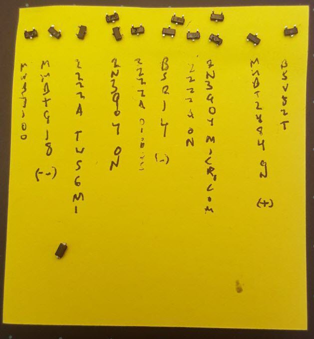
Note that the measurement limit for noise is around 70mVp-p, so some NPN transistors were possibly generating little to no noise. In general, it was observed that devices with higher breakdown voltages would generate more noise.
We settled on a 15V zener diode (MMSZ15T1G) as the initial device for noise generation. This device is squarely in the middle of the range of the TPS61158 regulator, is comfortably above the zener threshold, yet not excessively high (as a higher voltage would lead to higher power dissipation), and is guaranteed by the manufacturer to breakdown at a certain voltage. Although more noise was witnessed on a 24V breakdown device, operation near the cutoff threshold of the TPS61158 made the circuit unreliable under some startup conditions. Any lack in amplitude could be restored anyways by the follow-up signal conditioning circuitry.
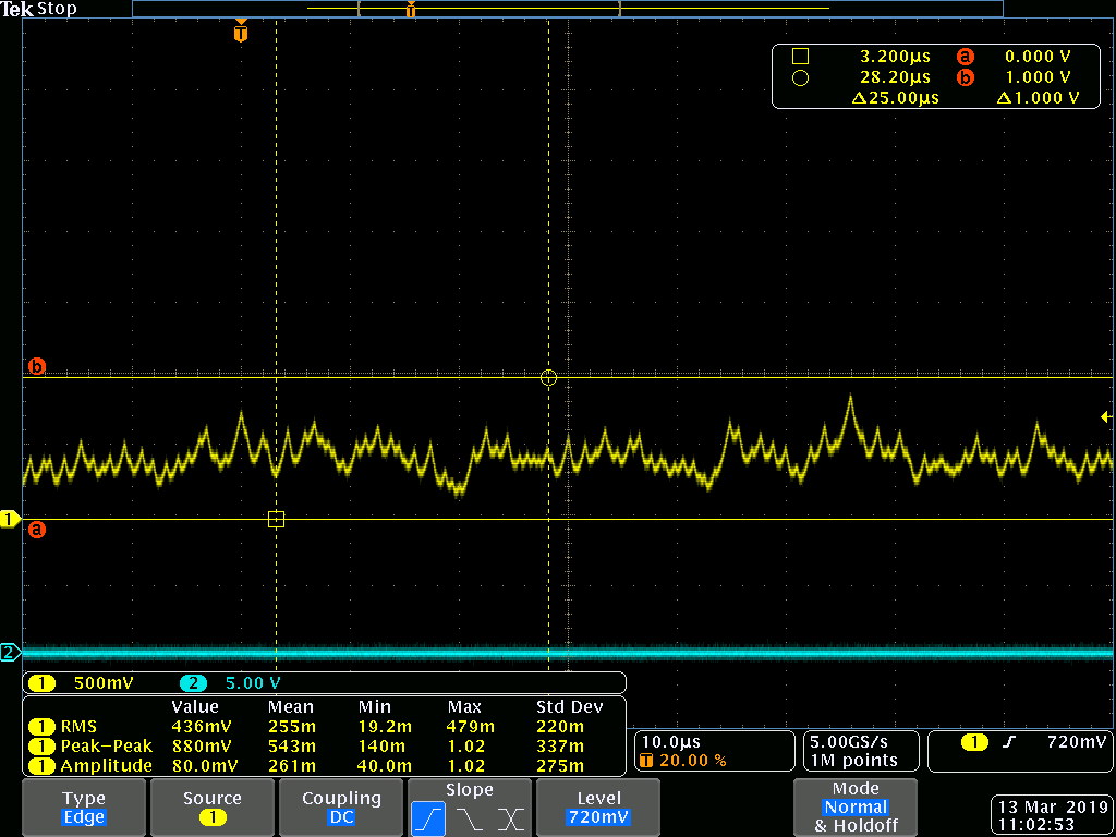
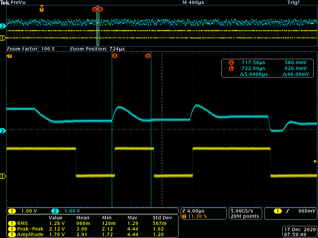
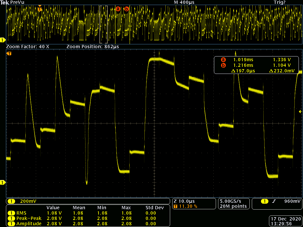
Above is the initial noise trace as measured by the circuit. One key observation is that the maximum frequency of the noise is quite high (» 1MHz), which leads to some bandwidth degradation as it feeds into the low-power op amp (GBW of 1.4 MHz).
The bandwidth of noise, and to a lesser extent the amplitude, can be tuned by placing a small capacitor in parallel with the avalanche junction. In this case, the MMSZ15T1G has about a 110pF or so depletion capacitance, so the parallel tuning capacitor should be sized around one order of magnitude larger. Basically what the parallel capacitor does is bleed away some of the current feeding into the junction, causing it to build up a field more slowly and thus reducing the bandwidth.
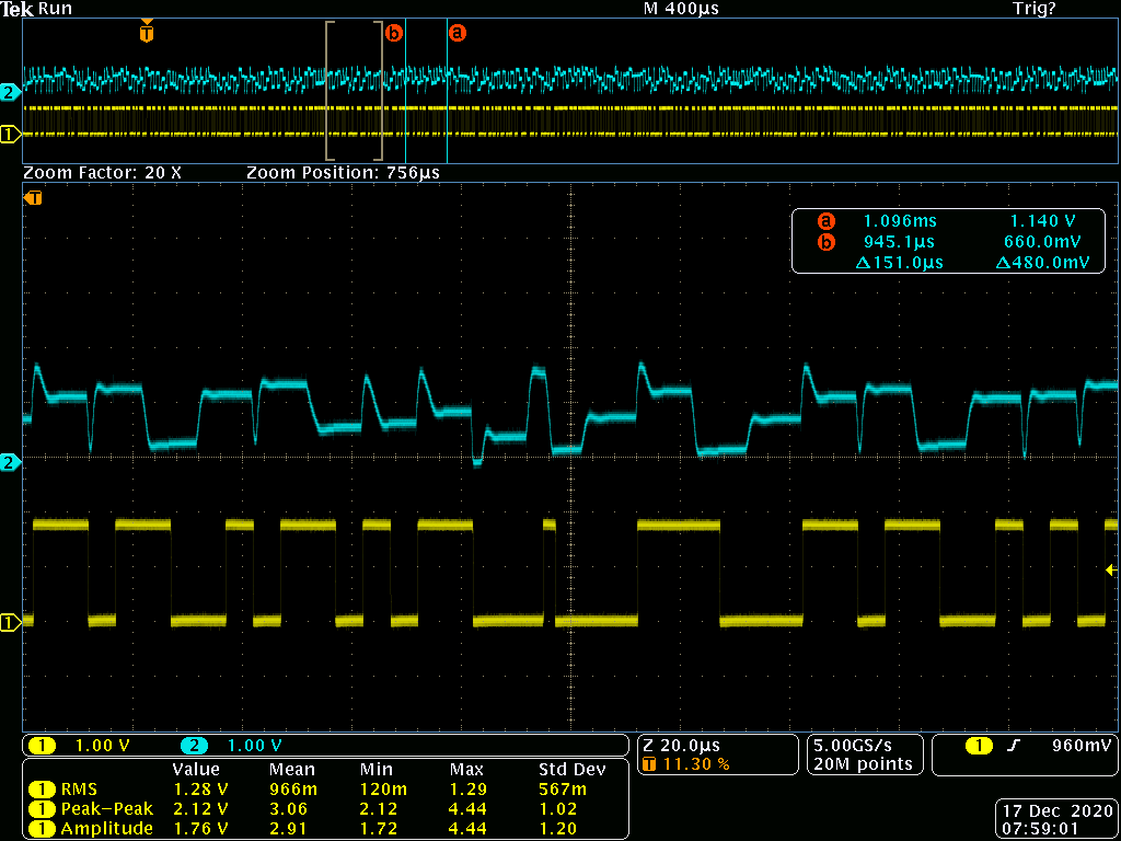
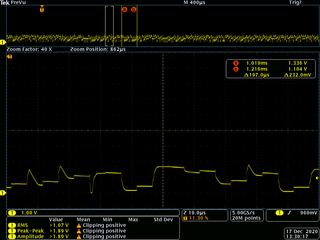
With a 1500pF capacitor placed in parallel with the noise source, we observe the following optimized noise trace, measured after the signal conditioning amplifier.
The noise in this case has a bandwidth that is suitable for sampling by the 1MSPS ADC, and the amplitude is close to 0-1V.
The optimized circuit has the following characteristics:
- 0.526mA @ 3.3V active current draw
- 0.0124mA @ 3.3V standby current draw (mostly LDO leakage, not shown in circuit)
- successfully boots at 2.8V and 4.4V
- generates noise at 0C and 80C. At 0C the noise is about 50% larger in amplitude, at 80C it’s about 50% smaller in amplitude.
Notes:
- The voltage on the regulation capacitor has a non-trivial amount of ripple. This probably applies a signature on the noise generated.
- The TPS61158 draws about 1uA through the feedback pin, which means of the target 4.2uA bias current, 1 uA is shunted into the feedback pin (resulting in 3.2uA going into the diode).
Next Iteration
The overall footprint is around 1 cm^2, and can be optimized further by going to a smaller inductor. The inductor initially chosen for the test circuit is greatly oversized for the application (just in case higher current were needed for testing). A much smaller inductor, perhaps an 0603 or 0805 part, could be used thus reducing the footprint even further. For example, a TDK MLZ1608M220WT000 is in an 0603 package and saturates at 55mA. This should be sufficient given the operating current of 3uA, although there is some question about the inductor’s performance during power-on.
A smaller footprint for the noise generating diode could be used as well. The initial layout used a SOT-23 footprint to accommodate a wide variety of devices but the final circuit could use a SOD-523. The following devices are candidates to be tested:
- BZT585B15T, BZT585B18T - zener diode, intended for voltage reference purposes
- PESD12VS1UB, PESD15VS1UB - TVS diode, intended for circuit protection
Modular Noise Generator
A design review had introduced the idea of the “modular noise generator” to me. This is, in theory, a noise source that is less sensitive to environmental factors like EM interference and temperature, and it has a very small start-up lag; in theory, it could be producing noise in dozens of microseconds, versus an avalanche generator which has to reach a certain fairly high voltage before it can function, a process that may take tens of milliseconds.
The modular noise generator is basically a modular voltage multiplier that attempts to continuously multiply the voltage stored on a capacitor, modulo the voltage rails. It can be thought of a successive approximation ADC (SAR ADC) that keeps approximating beyond the noise floor of the ADC. Consider, for example, a 12-bit ADC; it can’t meaningfully quantize anything beyond an SNR of 72.24dB. However, nothing stops you from running the 12-bit SAR ADC for four more cycles and getting a 16-bit result out of it; it’s just that the last 4 bits are all noise and functionally useless as far as an ADC. However, as a TRNG, those extra bits just keep getting better and better!
Thus, a modular noise generator is an “infinite-precision” SAR ADC made out of finite-precision parts; so, beyond the first dozen bits or so (which should be discarded), every successive bit that comes out of it should basically be a high quality entropy source.
Before committing to the avalanche generator, I decided to build a retrofit for the PVT version of Precursor (née Betrusted) that could drop a modular noise generator in place of the avalanche generator, so that I could evaluate its capabilities. The TL;DR is that we are still going with the avalanche generator, but I wanted to write up my findings with the noise source because it does have merit, but for various technical and project risk reasons I have decided not to adopt it.
Design
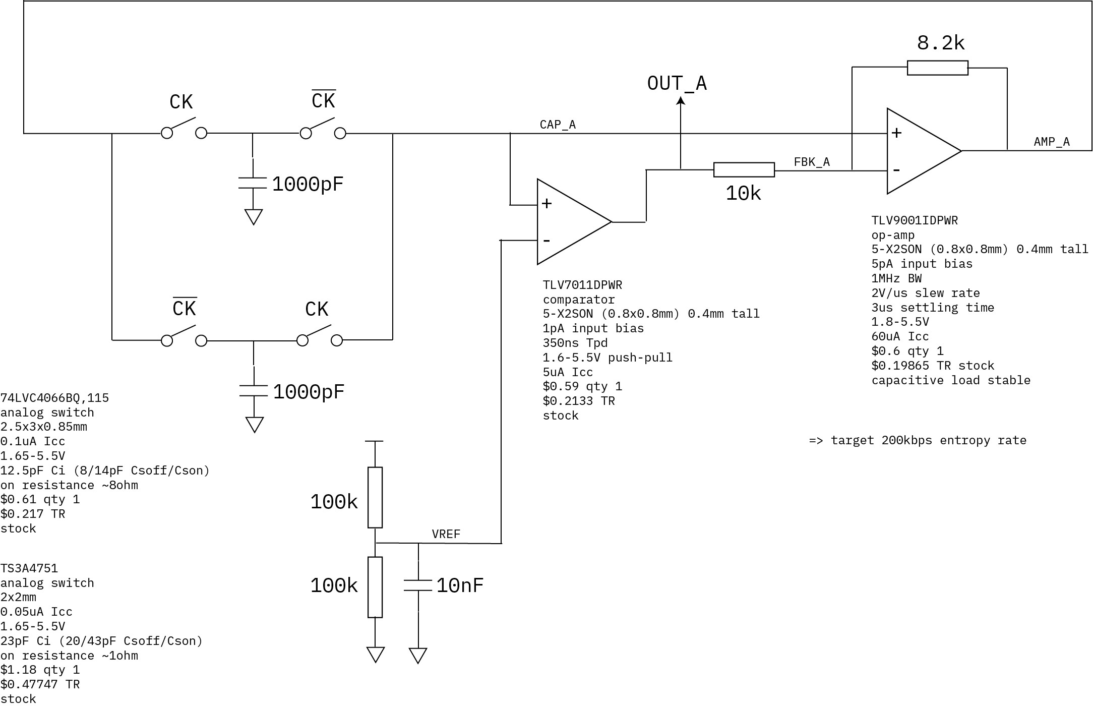
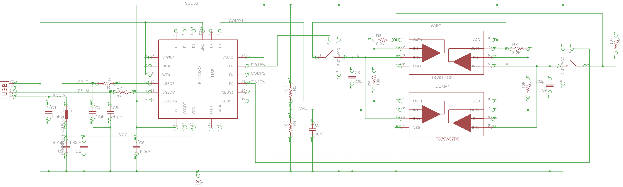
Above is a block diagram of the modular noise generator as implemented in the drop-in prototype. In a mobile device, power consumption and footprint are of paramount importance; thus, I took the original Infinite Noise Generator reference design and halved the number of devices required by multiplexing the comparator and op amp using an analog switch; notably, the design is already a switched-capacitor design that required analog switches, so the additional switches necessary to do the multiplexing come at virtually zero power and footprint cost.
The reference design has two op-amps, each consuming 0.6mA, and two comparators, each consuming 0.22mA, for a total of 1.64mA (typ quiescent) at 3.3V = 5.4mW, running at 300kbps. The avalanche generator, on the other hand, consumes 0.526mA (typ operational) at 3.3V = 1.7mW and generates entropy at rates at around 800kbps.
When comparing power numbers, note the following differences:
- 5.4mW for the modular noise generator is quiescent (idle, not generating noise)
- 1.7mW for the avalanche generator is on and generating noise
- The 7-series XADC power is not counted in the avalanche generator number; it’s already powered on for other uses. However, as a reference, the Vivado power estimator run on the actual design puts the power consumption of the XADC at about 1-2mW. Note this conflicts with the 34mW given by the 7-series “XPE” spreadsheet; I cannot find an explanation for this, but generally the output of the analysis tool is more accurate than the spreadsheet estimator.
While a few mW is only a tiny fraction of the “on” power of a Precursor, I felt that the modular noise generator had potential to operate at even lower powers.
By time-mutiplexing the op-amps and comparators, I’m able to halve the power consumption, and slightly reduce the footprint. By reducing the entropy rate to ~200kbps, I’m able to use lower-power devices, resulting in a current consumption of 65uA @ 1.8V (note the lower Vdd). At this power consumption, the bias resistors matter, so I add an extra 9uA for the Vref bias ladder for a total of 74uA @ 1.8V = 0.13mW. This power consumption is virtually negligible, and is small enough that power control to the generator is done by directly powering the op-amp and comparator off of an FPGA GPIO line.
If a higher entropy rate is desired, this could be accomplished by swapping out the TLV9001 op-amp for a pin-compatible TLV9061 device. The figure-of-merit to pay attention to is the settling time (ts) into a capacitive load, which is specified in the datasheets. The TLV9001 has a settling time of 2.5-3us at an Iq of 60uA; the TLV9061 has a settling time of 0.5-1us at an Iq of 538uA. Thus one can improve the speed of the generator by about 3x, at a roughly 7.5x increase in power.
The schematic as realized is shown above. Here are some notes about the implementation considerations:
- The decap (C1) for the op-amps is conservative because the power source is an FPGA I/O pin. It is a balance between decap performance and potentially damaging the FPGA I/O during the initial turn-on transient.
- Bigger resistors make more thermal noise, and consume less power, so the VREF for the comparator is derived from 100k resistors (instead of 10k). The downside is potential vulnerability to stray EM, but the 1000pF capacitor and careful layout helps mitigate that. It’s a balance between thermal noise generation and environmental sensitivity.
- We set the loop gain at 1.82, following the Infinite Noise Generator’s lead. The argument given is that by reducing the entropy from “perfect”, we can measure it. The intention is this source would be fed into a whitener after analysis. In practice, it also seems that a loop gain of 2.0 leads to the generator falling into stable states; likely due to hysteresis and component tolerances conspiring to stick it one way or the other. Thus there is some art in tuning the generator.
- The Infinite Noise Generator also has a 10k “mystery resistor” (R9 on its schematic) which I’m guessing is there to ensure that the generator always starts up, and does not get stuck in a stable state. In this design, the 1M dividers across the storage capacitors can be biased by changing out resistors, as necessary to ensure a positive startup condition.
- The load capacitors C3 and C4 are set at 1000pF so as to minimize the impact of charge sharing from the analog switch U3 (~12pF). The 74LVC4066B was picked over TS3A4751 primarily on the basis of the parasitic capacitance figure of merit. I replaced these with 100pF capacitors to see if it had a large impact on settling time; it did not, but there is a noticeable droop when the capacitor is in storage and a bump during switching transients, causing a significant reduction in entropy. Therefore, the larger capacitance is preferred. Note that the 1000pF capacitor is expected to contribute about 0.15mW of power (fsw * 0.5 * C * V2, fsw = 200kHz, C=1000pF, V = 1.8 * 0.707)
For the design as shown above to work, it’s crucial for clocks PHASE0 and PHASE1 to be non-overlapping. This ensures that there is no bleed-through of charge from CAP0 to CAP1. We use two GPIOs from the FPGA to generate non-overlapping clocks, which is fairly easy to do using a state machine and some counters.
I would like to point out that, like the avalanche generator, there is a vector for an attacker to bias the modular noise generator with a remote EM source. In the case of the avalanche generator, the possibility translates to introducing stray currents on the sensitive avalanche generator diode output, which operates at micro-ampere levels. These stray currents can imprint a repetitive or relatively fixed waveform superimposed on the noise waveform, which if a simple 1-bit discriminator is used, could result in the generator effectively being stuck in a single state. In the case of the modular noise generator, it’s argued that the modular noise amplifier simply amplifies all the noise, and does not care if it comes from shot noise, EM, thermal, cross-talk. However, if an attacker can correlate its EM timing to that of the modular noise generator’s period, it may be able to influence the voltage reference for the comparator. Stray currents introduced onto this node can repetitively influence the “decision” of the comparator one way or the other, causing the entropy to gain a correlation to an external EM field, such that the modular noise generator eventually enters a “stuck” state. Thus, both generators have a potential remote EM influence threat, but both generators also have correspondingly trivial mitigations to this.
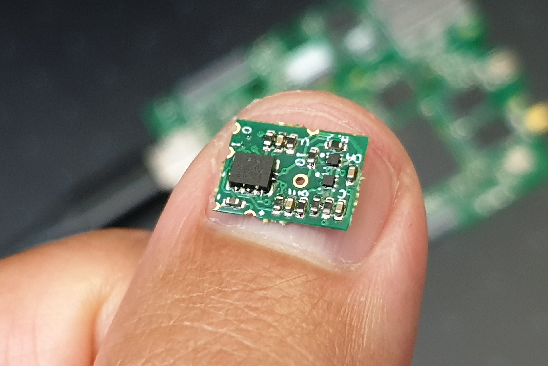
Above is the evaluation module as assembled, pictured on top of a thumb nail.
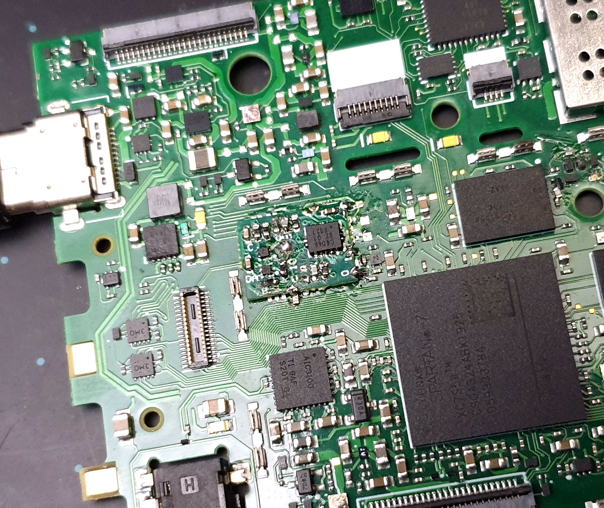
Above is the evaluation module mounted onto a Precursor. Castellations on the edge of the board plus one through-hole are used to contact existing points used in the existing avalanche generator, which are then re-purposed to drive the modular noise generator through the magic of FPGAs.
The astute observer will note the random resistor hanging off of a solder pad on the bottom edge of the carrier board, that’s just a technique I use to “save” components when swapping stuff out to try different things, as a component tacked onto a pad has minimal parasitic effect on the circuit.
Characterization
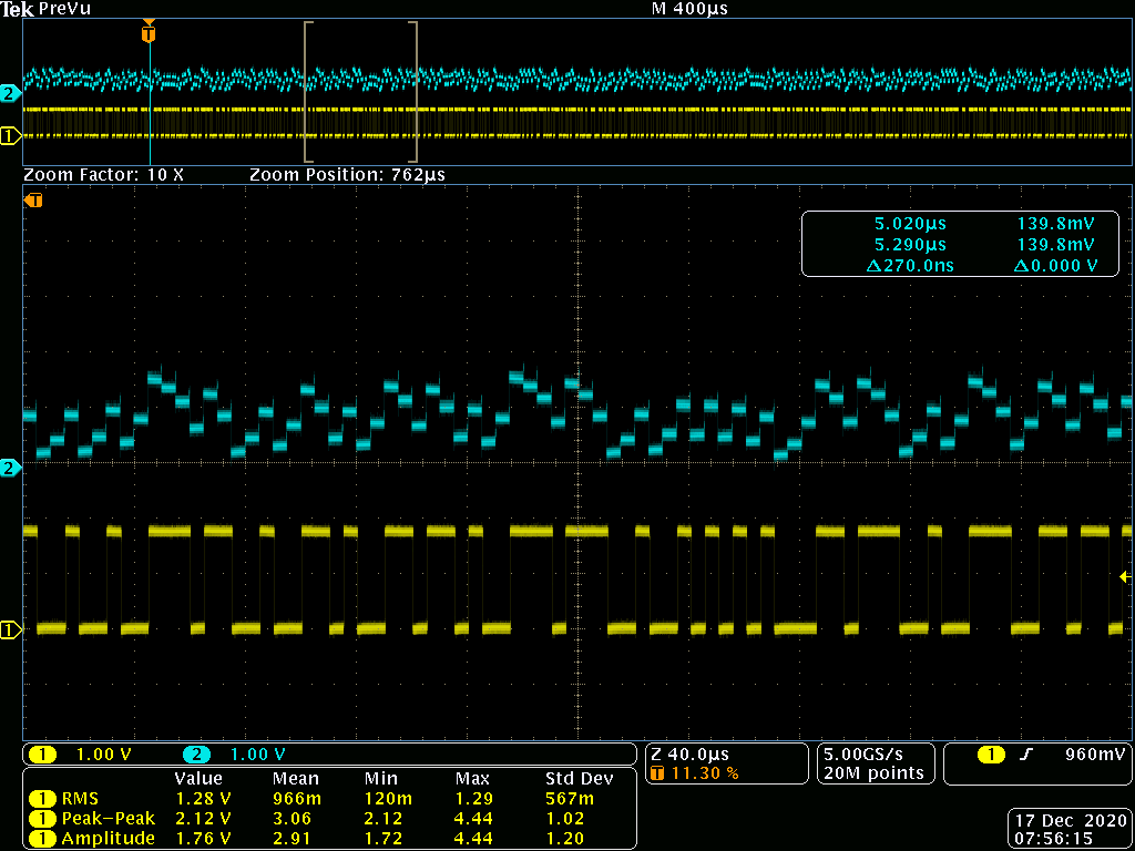
The following diagrams are made with the modular noise generator “as designed” (gain=1.82, Cl=1000pF) unless otherwise noted. The FPGA is generating non-overlapping clocks with a period of ~5us, with a 50ns non-overlap dead time in between each phase as seen below:
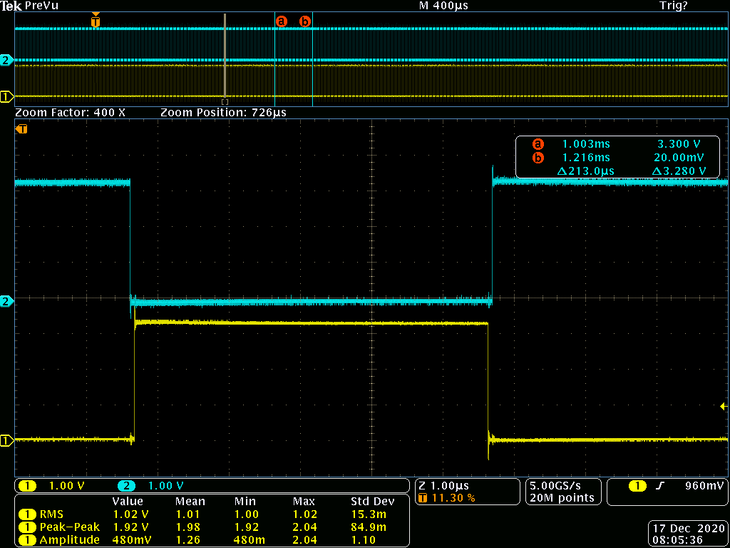
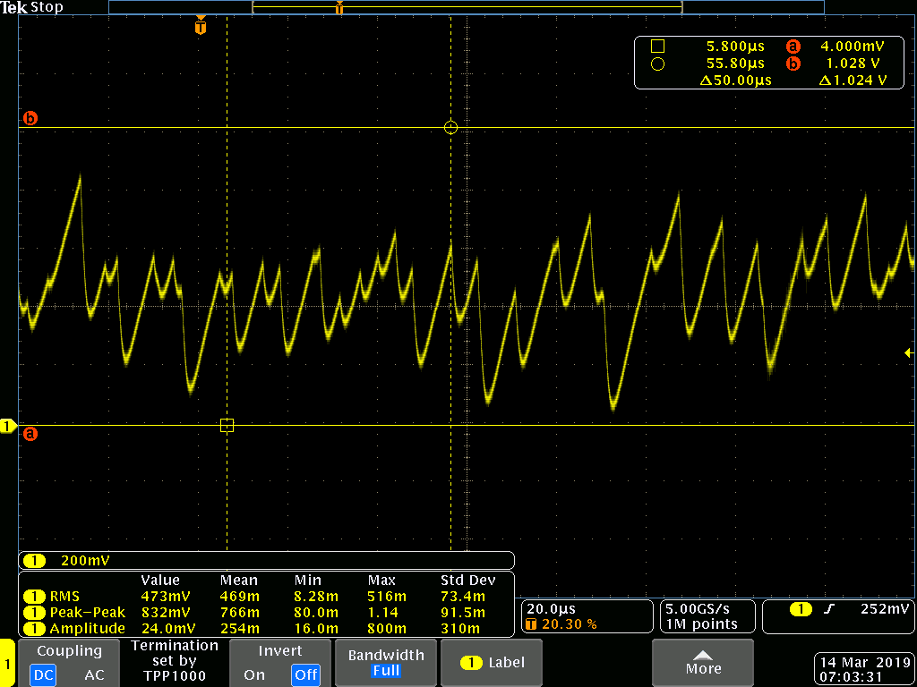
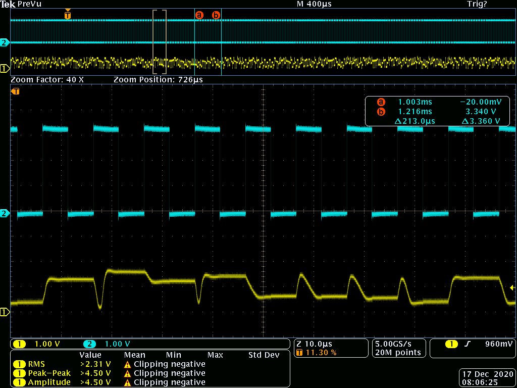
Below is probably the most illuminating image detailing how the design functions. The yellow trace is CAP1, and the cyan trace is CAP_A. As you can see, CAP_A assumes a new value at twice the rate of CAP1, as it is the output after the analog switches that interleave between the two capacitors. The CAP_A node is nice and crisp, as expected. The CAP1 node shows the settling time of the op-amp: as the op-amp is multiplexed between between two capacitors, half the time the capacitor is driven by the op-amp, and the other half of the time it’s being “read out” as the input to the op-amp. One can see that the op-amp uses up almost all of the allotted 5us to settle to its final value. Experiments to reduce the settling time indicate this is about as fast as you can realistically run the circuit with this op-amp; if the period is shortened, the generator ends up in a stable state.
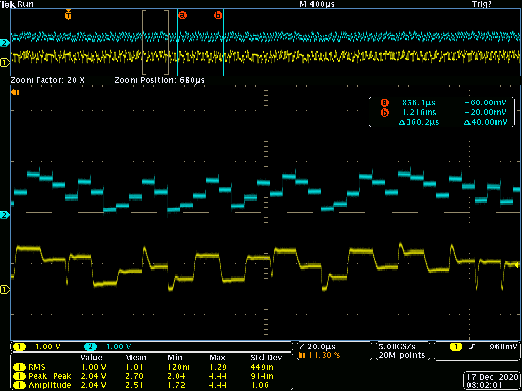
The image below compares the value on CAP1 (cyan) to the output of the TRNG (yellow).
Below zooms in more to focus on the settling time of the op-amp into the capacitor.
Below shows the output of the TRNG compared to the voltage on the CAPA node. If you draw an imaginary line at VDD/2 through the cyan trace, you get the yellow trace.
Below compares a non-overlapping clock phase to CAP1. Here you can see how when the phase is driven high, the capacitor is engaged to the op-amp and it changes value; and when it is low, it’s isolated and suitable for readout.
Below are images showing what happens when a 100pF capacitor is used instead of a 100pF capacitor for storage. The scale is exaggerated on the second image so that the droop issues are clearly visible.
It’s expected that this noise source should fall short of generating 1 bit of entropy per bit (should be 0.86). I did a short data collection run, and here are the initial results.
ent returns the following values:
Entropy = 7.847409 bits per byte.
Entropy = 7.847957 bits per byte.
Entropy = 7.847004 bits per byte.
Which is about 0.98 bits of entropy per bit. Dieharder’s birthdays also flags this reduction of entropy:
diehard_birthdays| 0| 100| 100|0.00006712| WEAK
The higher-than-expected performance is probably due to the fact that this characterization run was only considering the output of one phase of the modular multiplier, and therefore the bitrate was half of the expected value and we’re throwing away every other sample.
For the next data collection run, I increased the loop gain to 1.92,
which should improve entropy to about 0.93 bits per bit. This was done
by changing out the gain resistor R5 to 9.1k. Note that this change
initially caused the modular noise generator to get stuck in a stable
state, so that the output was stuck at 1. Removing R7 forced a
bias onto one of the storage caps, which pushed the generator into
the desired metastable state.
In this run, we also correct the sampling rate error, so it’s a little hard to compare to the previous data.
ent returns the following values:
Entropy = 7.541152 bits per byte.
Entropy = 7.547037 bits per byte.
Entropy = 7.542359 bits per byte.
Which is about 0.945 bits per bit of entropy, and closer to the expected result of 0.93 bits per bit.
Dieharder is not at all happy about the reduction in entropy:
diehard_birthdays| 0| 100| 100|0.00000000| FAILED
Conclusions
The modular noise source is a compact, low power noise source. The design as evaluated produced a reduce rate of entropy, but had very good power numbers. As expected, the design does not produce a full bit of entropy per bit, and attempts to coax it into the realm of producing full entropy revealed that the design is liable to fall into stable states when the entropy rate is too high.
When compared to the existing avalanche generator, we find that:
- Area: the modular noise generator is slightly smaller
- Power: avalanche = 1.7mW; modular noise generator can reduce to as little as 0.13mW, but practically speaking we’d tune the generator to ~1mW for greater entropy rates. So the power is about the same, and either way, negligible compared to the system.
- Entropy rate: at 0.13mW, we generate ~200kbps of entropy per second; at 1mW we may be able to improve that to 400-500kbps. Avalanche can generate about 800kbps.
- Entropy quality: modular noise generator outputs ~0.86-0.95 bits of entropy. Avalanche generator outputs close to 1.0 bits of entropy per bit at full rate without an additional whitener.
- Stability: the reduced entropy of the modular noise generator is necessitated by the fact that it falls into stable (e.g. constant output) states if the entropy rate gets too high. On the other hand, the avalanche effect is empirically determined to be robust so long as the bias voltage is high enough, and the temperature is lower than 80C.
- Startup lag: in the modular noise generator, the first 20-30 bits of entropy are not usable, so the startup lag is about 0.15ms. The avalanche generator requires a high-voltage regulator to stabilize, which takes about 20-50ms.
Thus, while the modular noise generator can improve on area and power, from a system engineering perspective, these are not significant compared to the rest of Precursor. Entropy rate generation, while inferior, is probably acceptable from a system design standpoint.
For Precursor, the greatest system-level concerns are around entropy quality and stability. The argument in favor of the modular noise source is that the controllable entropy quality of the modular noise source is a feature, not a bug – an entropy of ~0.9 bits per bit is low enough to be extracted with a simple, quick test, as opposed to the typical challenge of collecting gigabytes of entropy on a typical TRNG to uncover subtle biases. This has the potential to allow for simple and fast verification that the device is working correctly. Furthermore, all entropy sources in Precursor will be coupled, in software, with an optional cryptographic whitening function for defense-in-depth, so a slightly reduced source entropy won’t have a meaningful impact on the final application entropy.
This argument may have some merit, however, I hypothesize that the deliberate reduction in entropy to facilitate metrology is probably difficult to differentiate from hostile reductions in entropy from attackers. It’s an open area of research if this reduction in entropy can be safely and robustly used to characterize the performance of an entropy source. I suspect it can be; however, it would be several months of focused research to prove it can be.
Thus the biggest concern I have with dropping the modular noise generator into the design at the 11th hour is the observed behavior of the noise generator falling into stable states. The results reported in the analysis above are always done after some bodges to work around any stable states that were encountered. Some tests even show the generator phasing in and out of a stuck-1 or -0 condition. I suspect the main culprits are probably the hysteresis of the comparator, plus component tolerances that tend to bias/stack the result in a particular direction.
That I cannot ascribe an analytical solution to this is problematic, and it’s especially problematic if the situation is aggravated by corner cases in the analog component tolerances – determining the extent of this sensitivity might only come out in mass production, at which point it’s too late to fix. To arrive at a robust answer to this would be a several month’s effort at a minimum. Notably in the context of this project, the avalanche generator has already been scrutinized for several months, unlike the modular noise generator.
I don’t think it’s worth it to delay the delivery of Precursor by several months while we prototype and confirm its robustness. Thus, the modular noise generator is not swapped into the Precursor design, and we stay with the avalanche generator.
For completeness, here are the the primary concerns raised around using the avalanche generator, and the corresponding mitigations deployed:
- Avalanche generators could be vulnerable to remote EM injection attacks, where an adversary attempts to influence the output of the generator by irradiating the target with radio waves of sufficient power to swamp out the noise created by the avalanche diode. In Precursor, this is mitigated by putting a robust Faraday cage around the trusted domain; the amount of power required to induce this failure is probably high enough that it would damage other circuits and/or cause physical injury to nearby people. Compact circuit layouts like that employed in Precursor are also less sensitive to external noise, because the area of the loop to capture external field fluxes is that much smaller.
- Some avalanche generators are known to be vulnerable to aging, but this is, at least anecdotally, linked to the use of NPN transistors as avalanche generators. In Precursor, we use a higher-voltage diode whose junction was explicitly engineered for the purpose of long-term operation in an avalanche mode.
- Avalanche generators have an entropy output that changes with temperature. However, Precursor is engineered to produce sufficient output amplitude across a range from 0-80C. Note that above 60C, the device becomes literally too hot to handle.
Furthermore, there is a system-level concern around the startup lag of the avalanche generator. This is mitigated in part by a 32 kilobit deep hardware FIFO that auto-refills once it falls below 50% in the FPGA; under most real-world usage situations, the startup lag would never be a factor.
In short, the potential drawbacks of using the avalanche generator are largely mitigated through additional design features in Precursor. Thus we are sticking with it for production because it is well-characterized, and the impact of material variation on its performance is better understood than the potential impact of material variation on the modular noise generator.
Navigation
- Betrusted
- HCI Rationale
- Betrusted Architecture
- Development Plan
- Avalanche Noise Source Design